Register Transfer Language
In symbolic notation, it is used to describe the micro-operation transfers among registers. It is a kind of intermediate representation (IR) that is very close to assembly language, such as that used in a compiler. The term "Register Transfer" refers to performing micro-operations and transferring the result of an operation to the same or another register.
Register Transfer Language (RTL) is a low-level language used to describe the functioning of a digital circuit and, more specifically, the transfer of information between registers. It illustrates how data moves from one register to another and how data is processed within the digital system. RTL enables the creation of abstraction levels where high-level design descriptions can be linked to low-level hardware implementations in the design, simulation, and synthesis of digital circuits.
- RTL provides meaningful descriptions of the flow of data between hardware registers.
- It is applied to the representation of synchronous circuits—circuits controlled by clock signals.
- It describes the transfer of data and logical operations at the register level.
- RTL designs are typically documented using hardware description languages like Verilog or VHDL.
- It serves as an abstraction layer between high-level Application-Specific Integrated Circuits (ASICs) and physical devices.
Usage of RTL in digital design
- Describes the behavior of hardware at the register-transfer level.
- Used to model data flow using registers.
- Assists in the transition from conceptual to gate-level designs.
- Allows simulation and validation of the hardware’s behavior.
- Serves as the foundation for circuit development using HDLs.
In the statement:
R2 <- R1the arrow <- acts as a replacement operator. This statement defines the transfer of the content of register R1 into register R2.
Methods of RTL representation:
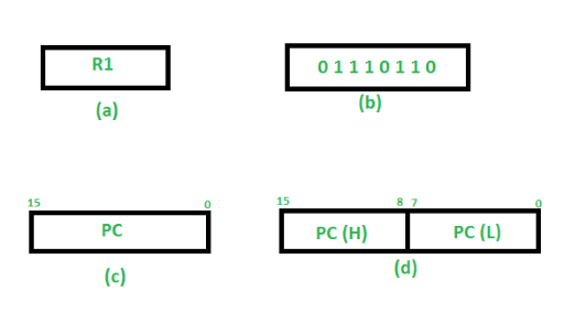
- A register is generally represented by its name enclosed in a rectangular box, as shown in (a).
- Registers are numbered sequentially from 0 to (n-1), as shown in (b).
- The bit positions in a register can be marked on top of the box, as shown in (c).
- A 16-bit register PC can be divided into two parts—bits (0 to 7) are assigned to the lower byte of the address and bits (8 to 15) to the higher byte, as shown in (d).
Basic symbols of RTL
| Symbol | Description | Example |
|---|---|---|
| Letters and Numbers | Denotes a Register | MAR, R1, R2 |
| Denotes a part of register | R1(8-bit) R1(0-7) | |
| Denotes a transfer of information | R2 R1 | |
| Specifies two micro-operations of register transfer | R1 R2, R2 R1 if P = 1 | |
| Denotes an additional name for an already existing register/alias | Ra := R1 |
Advantages of Register Transfer Language (RTL)
- Enables efficient hardware design.
- Allows simulation and early detection of potential errors.
- Implements conceptual descriptions down to gate-level hardware.
- Facilitates design component reuse.
- Provides a clear framework for timing analysis.
Disadvantages of Register Transfer Language (RTL)
- Despite high performance, debugging can be challenging.
- May lead to inefficient, bulky designs if not optimized.
- Its hardware-oriented nature may be difficult to grasp without understanding data flow.
- Synthesis results depend on specific tool capabilities.
- Offers lower abstraction compared to high-level descriptions.
Register Transfer
The transfer of information from one register to another, represented symbolically using a replacement operator, is called Register Transfer.
Operations performed on data stored in registers are referred to as register transfer operations.
Types of Register Transfer Operations:
-
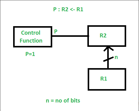
Simple Transfer The contents of R1 are copied into R2 without affecting R1. This is an unconditional transfer.
R2 <- R1 -
Conditional Transfer
If P = 1, then the content of R1 is transferred to R2. This is a unidirectional operation.
-
Simultaneous Operations When two or more operations occur simultaneously, they are separated by a comma (,).
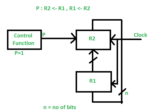
If the control function P=1, then load the content of R1 into R2 and at the same clock load the content of R2 into R1.
Bus & Memory Transfer
Bus Memory Transfer
A bus transfer is an effective method to send data using a common bus system. It is constructed using shared bus lines connected to multiple registers. The bus mechanism includes a collection of lines, each being one bit wide, which can carry only one piece of information at a time. Data transfer is controlled by control signals.
The two methods used in bus transfer are as follows:
- Using a multiplexer
- Using three-state bus buffers
Using Multiplexer
A common bus can be implemented using a multiplexer. It facilitates the selection of a source register to place binary data on the bus. The bus register has input and output gating controlled by control signals. The diagram demonstrates the input and output gating of registers.
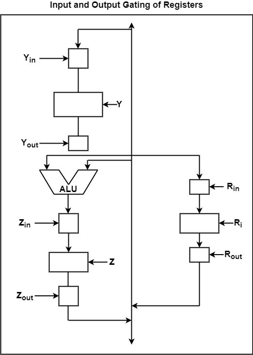
- Ri is a register, and Rin and Rout are the input and output gating signals of Ri.
- Z is a register, and Zin and Zout are the input and output gating signals of register Z.
- Y is a register, and Yin and Yout are the input and output signals of Y.
The figure shows the input and output gating. The switches are controlled by control signals. Rin and Rout are the input and output gating signals of register Ri. When the signal is ON, Ri is set to 1; when the signal is OFF, Ri is set to 0.
When the input gating Rin is set to 1, data is loaded into register Ri via the common bus. When Rout is set to 1, the contents of register Ri are placed on the data bus. These are referred to as input-enabled and output-enabled signals. The operations that take place inside the processor are synchronized with the clock pulse.
Three-State Buffers
Three-state buffers can also be used to implement a common bus. A buffer is a memory area inserted between devices to manage communication and ensure proper interfacing. It operates in three states: 1, 0, and high-impedance. These three states are defined as follows:
- Logic 0 and 1 are conventional logic states.
- The high-impedance state means the output is effectively disconnected and has no logic value.
- These three-state gates can implement standard logic functions such as AND, NAND, OR, and NOR.
The diagram demonstrates the logic symbols and the associated truth table.
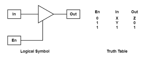
As shown in the figure:
- When the control input is 1, the output is enabled, and the gate functions as a buffer, passing the input to the output.
- When the control input is 0, the gate enters a high-impedance state (Z), and the output is disabled.
- The impedance in three-state buffers allows all outputs to be connected to a single bus line without causing conflicts.
- The truth table shows that when the gate is disabled, the output enters a high-impedance state regardless of the input.
- When the gate is enabled and an input is provided, the output reflects the input.
- When the gate is enabled and the input is 1, the output is 1.
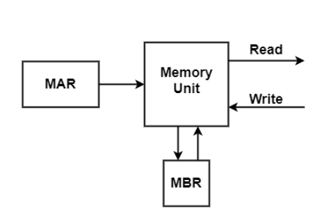
Memory Transfer
The transfer of data from a memory word to the external environment is called a read operation. In a memory transfer, the read operation involves transferring data from the memory word selected by the address register (AR) into the memory buffer register (MBR).
[AR]M → MBR = Read Operation
The read control signal initiates this process. The read statement generates data transfer from the selected memory register M to the MBR.
The transfer of new data to be stored in memory is called a write operation. In a write operation, data is transferred from the memory buffer register (MBR) to the memory location pointed to by the address register (AR).
MBR → M[AR] = Write Operation
The write control signal initiates the write operation. The write statement causes data transfer from the MBR to the memory location addressed by M[AR].
To perform a read or write operation, the memory register M must first be selected using a specific address.
The figure shows a representation of memory transfer. It demonstrates that the memory unit can transfer data using the address register (AR) and the memory buffer register (MBR) to execute read and write operations.
Advantages:
- Simpler and Inexpensive Design: A single bus structure is easy to implement and relatively inexpensive, making it suitable for smaller or simpler systems.
- Efficient Resource Utilization: Bus arbitration ensures fair access to the bus, preventing any single device from monopolizing it and causing system slowdowns.
- Support for Multiple Devices: A shared bus allows multiple devices, such as I/O peripherals, to communicate with the CPU and memory.
- Easy Memory Access: The address bus enables straightforward memory access, with the CPU sending the address and data to the required memory location.
- Scalability: The bus structure can be expanded to accommodate more devices as needed.
Disadvantages:
- Limited Data Transfer Speed: A single bus can become a bottleneck, especially when multiple devices require simultaneous data transfers.
- Potential for Bottlenecks: If a large volume of data must be transferred, the bus may become saturated, reducing system performance.
- Bus Contention: Multiple devices requesting bus access at the same time can lead to conflicts and delays.
- Complexity with High-Speed Transfers: As data transfer rates increase, the bus structure becomes more complex, requiring advanced arbitration and control mechanisms.
- Need for Bus Arbitration: Arbitration logic is needed to manage bus access, adding to system overhead and complexity.
Logic Micro-Operations
Logic operations are binary micro-operations implemented on the bits stored in registers. These operations treat each bit independently and treat them as binary variables.
For example, the exclusive-OR micro-operation between the contents of two registers R1 and R2 is denoted by:
P: R1 ← R1 ⊕ R2
This represents a logic micro-operation applied to each bit of the registers, assuming the control variable P = 1. Suppose each register has four bits. Let the content of R1 be 1010 and R2 be 1100.
The exclusive-OR operation results in:
1010   Content of R1
1100   Content of R2
0110   Content of R1 after P = 1
The contents of R1 after the operation reflect the bitwise exclusive-OR between R2 and the original R1.
Special Symbols
Special symbols are used for logic micro-operations (OR, AND, and complement) to distinguish them from similar Boolean function symbols. The symbol V is used for OR micro-operation, and a dot (•) or juxtaposition can be used for AND micro-operation.
The complement micro-operation corresponds to 1’s complement and is represented with a bar over the register symbol. These different symbols help differentiate between logic micro-operations and Boolean expressions or control functions.
There is a reason for using two sets of symbols—to distinguish between arithmetic and logic operations. For example, the symbol + can represent either arithmetic addition or logical OR. Its meaning depends on the context:
- When + appears in a micro-operation, it indicates arithmetic addition.
- When + appears in a control or Boolean function, it indicates a logical OR.
We do not use + to denote a logic micro-operation.
For example:
P + Q: R1 ← R2 + R3, R4 ← R5 V R6
Here:
- P + Q is a Boolean expression (OR between two control signals).
- R2 + R3 is an arithmetic addition.
- R5 V R6 is a logic OR micro-operation.
Shift Micro-Operations
Shift micro-operations are used for serial data transfer and are often used with arithmetic, logic, and data-processing operations. The contents of a register can be shifted left or right.
As the bits are shifted, the first flip-flop takes input from the serial input. In a shift-left operation, the serial input provides a bit to the rightmost position. In a shift-right operation, it provides a bit to the leftmost position. The data from the serial input determines the type of shift.
Types of Shift Micro-operations
There are three types of shift micro-operations:
Logical Shift
In a logical shift, 0 is transferred through the serial input.
shlis used for logical shift leftshris used for logical shift right
R1 ← R1 shl R1
R2 ← R2 shr R2
The same register should be on both sides of the operation.
Circular Shift
In a circular shift, bits rotate around the two ends without data loss. The serial output of the shift register is connected back to its serial input.
cilis used for circular shift leftciris used for circular shift right
The symbolic notation for these operations is shown in the table.
| Symbolic Designation | Description |
|---|---|
| R R1 shl R | Shift-left register R |
| R R1 shr R | Shift-right register R |
| R R1 cil R | Circular shift-left register R |
| R R1 cir R | Circular shift-right register R |
| R R1 ashl R | Arithmetic shift-left R |
| R R1 ashr R | Arithmetic shift-right R |
Arithmetic Shift
An arithmetic shift shifts signed binary numbers left or right:
- An arithmetic shift left multiplies the number by 2.
- An arithmetic shift right divides the number by 2.
The arithmetic shift keeps the sign bit unchanged to preserve the number’s value.
| R | R | R | R | R |
|---|
Arithmetic Shift Right
In this case:
- The leftmost bit (Rn-1) is the sign bit (0 for positive, 1 for negative, using 2’s complement form).
- Bit Rn-2 is the most significant bit of the number.
- R0 is the least significant bit.
During an arithmetic shift right:
- The sign bit Rn-1 remains unchanged.
- Rn-2 receives the bit from Rn-1, and so on for the rest of the bits.
- The bit in R0 is discarded.
Computer Architecture & Organisation
CSPC-313 Computer Architecture & Organisation HPTU BTech CSE Syllabus
Basic Computer Organization
Instruction codes, computer instructions, timing & control, instruction cycles, memory reference instruction, input/output & interrupts, complete computer description & design of basic computer.